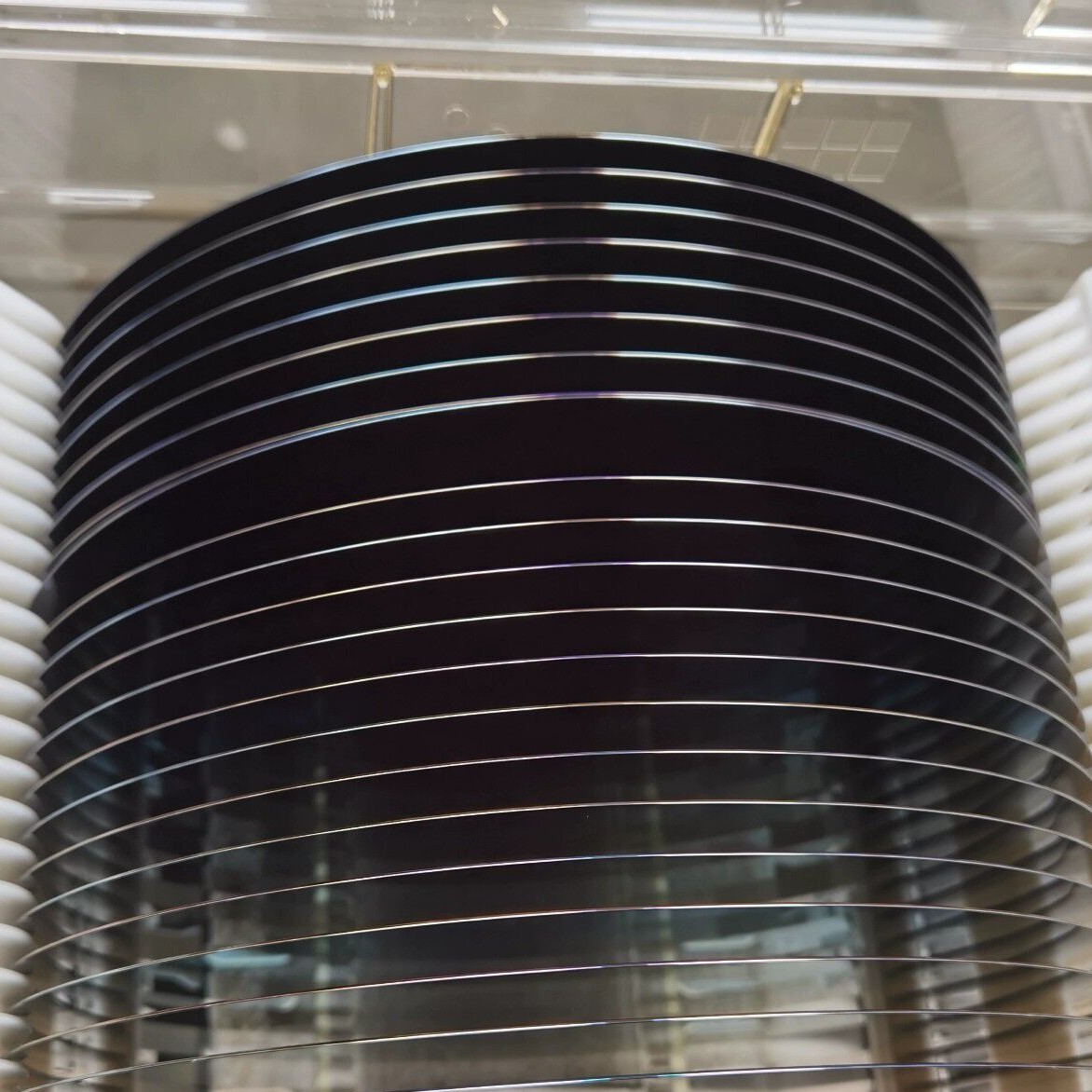
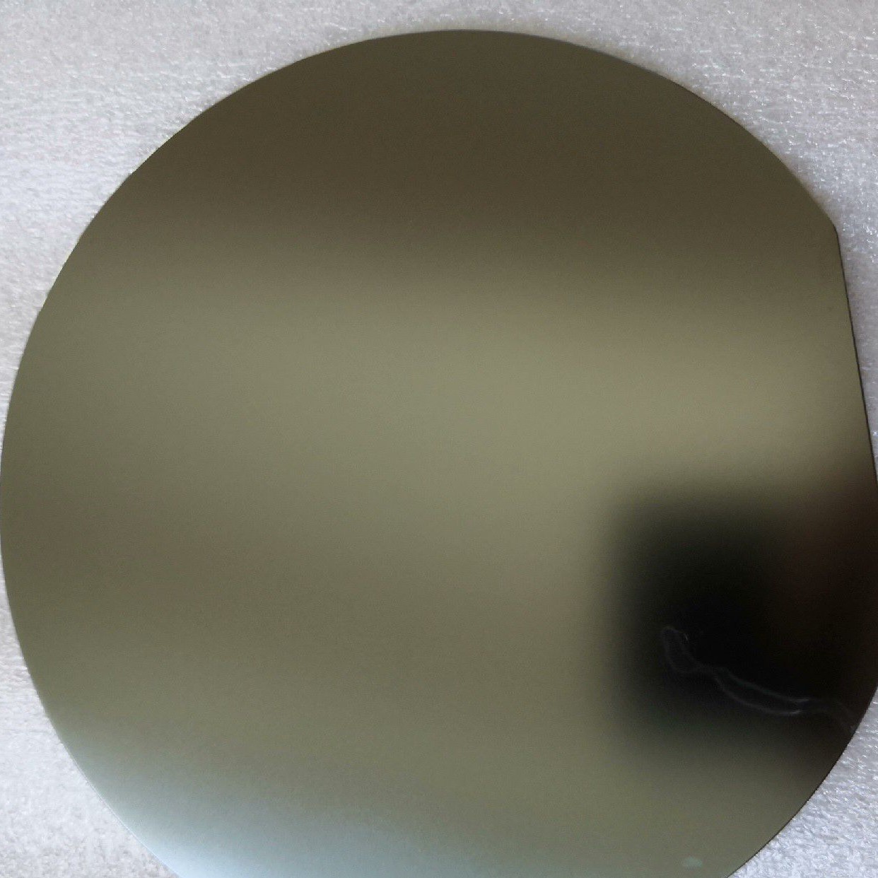
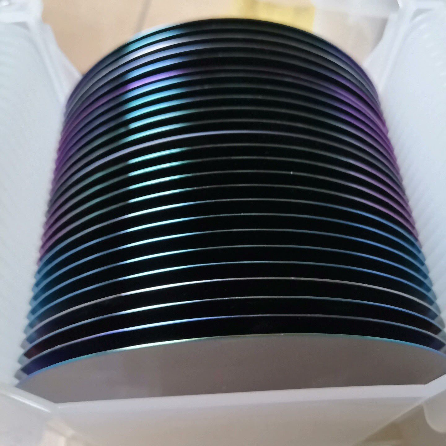

| Diameter | 2" | 3" | 4" | 5" | 6" | 8" |
| Growth Method | CZ,FZ | |||||
| Orientation | < 100 > , < 111 > , < 110 > | |||||
| Type/Dopant | Intrinsic, N Type/Phos, P Type/Boron | |||||
| Thickness (um) | 279 | 380 | 525 | 625 | 675 | 725 |
| Thickness Tolerance | Standard ± 25um | ±50um | ||||
| Resistivity(Ohm-cm) | >1000Ω.cm,>3000Ω.cm,>5000Ω.cm,>10000Ω.cm,>20000Ω.cm | |||||
| Surface Finished | P/E , P/P, E/E, G/G | |||||
| TTV (um) | Standard < 10 um | |||||
| Bow/Warp (um) | Standard <40 um | <50um | ||||
| Particle | <10@0.3um | |||||
Can be customized according to your requirement.sales@hr-optics.com
He Rui Optics produces a variety of precision optical components with experienced engineers and advanced equipment.We can produce standard and customized optical lens,mirror,filter,prism,windows,crystal,wafers.If you have any requirement,please contact us
Tags: Optical Lenses Optical windows Optical Prisms Optical filters Optical Mirrors Optical Crystals Silicon Wafers Silicon lens cylindrical lenses laser optics infrared optics uv optics


 Send Email
 售前客服
售前客服