| Crystal Materials | 99,999%, High Purity, Monocrystalline Al2O3 | |
| Grade | Prime, Epi-Ready | |
| Surface Orientation | C-plane, A-plane, R-plane, M-plane, N-plane, V-plane, 10-14, etc.) and, with a miscut if desired. | |
| C-plane off-angle toward M-axis 0.2 +/- 0.1° | ||
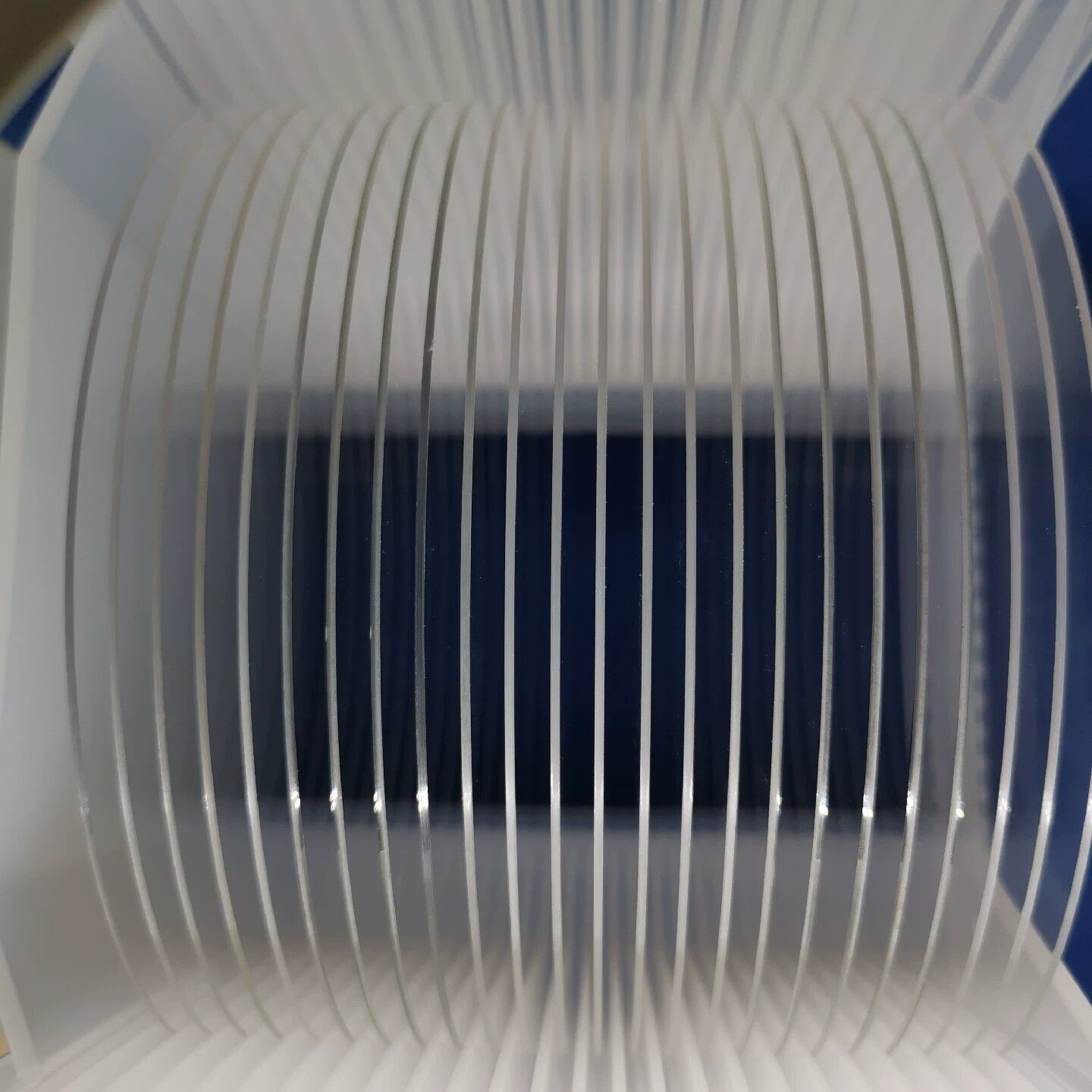
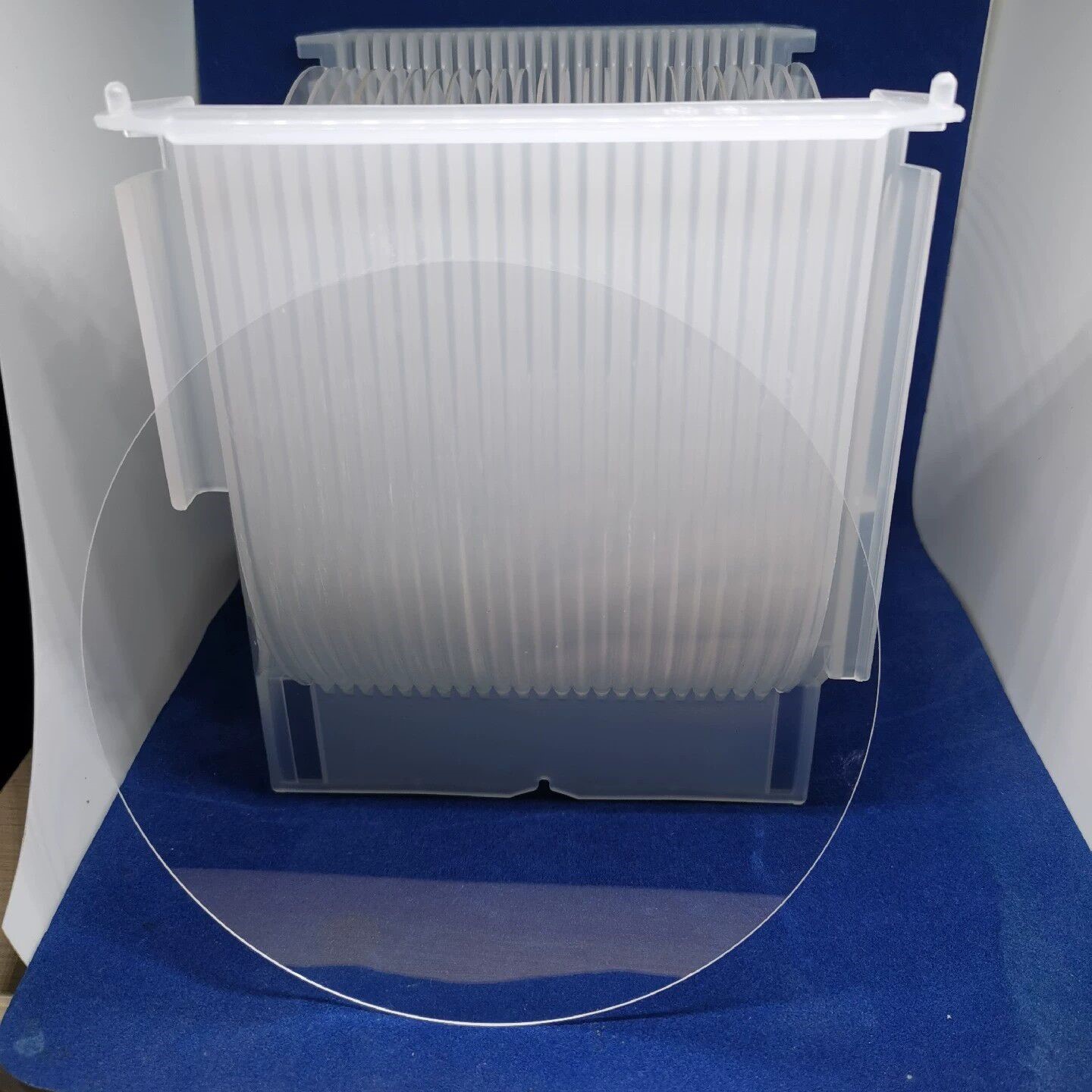
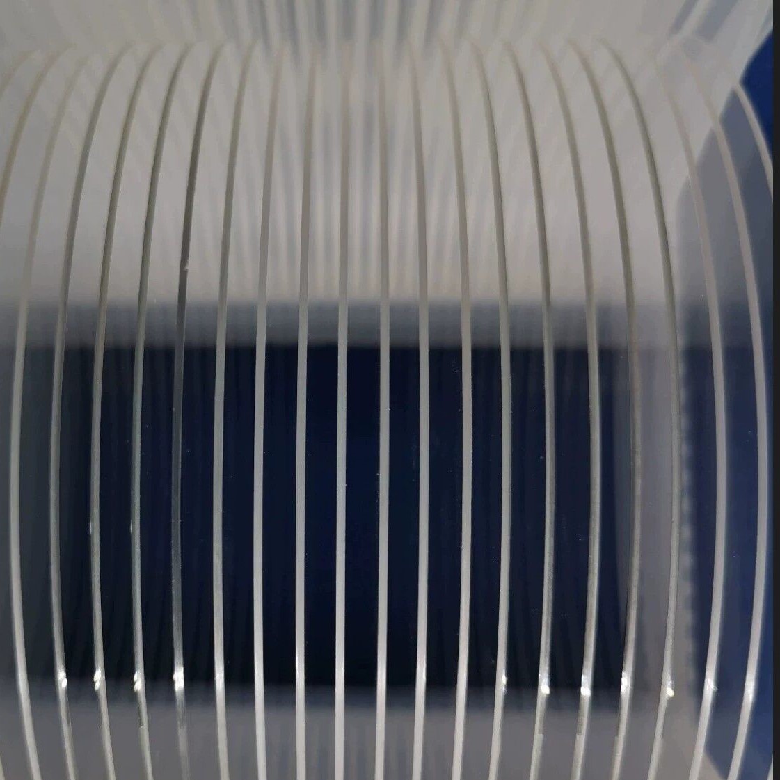
| Diameter | 1'' 2'' 3'' 4'' 5'' 6'' 8'' +/- 0.1 mm | |
| Thickness | 100um、280um、300um、350um、400um,430um、500um、600um,650um,1300um,1mm+/- 25 um | |
| Single Side Polished | Front Surface | Epi-polished, Ra < 0.2 nm (by AFM) |
| (SSP) | Back Surface | Fine ground, Ra = 0.8 um to 1.2 um |
| Double Side Polished | Front Surface | Epi-polished, Ra < 0.2 nm (by AFM) |
| (DSP) | Back Surface | Epi-polished, Ra < 0.2 nm (by AFM) |
| TTV | < 5 um | |
| BOW | < 5 um | |
| WARP | < 5 um | |
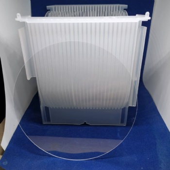
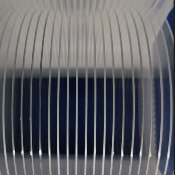
| Cleaning / Packaging | Class 100 cleanroom cleaning and vacuum packaging, | |
| 25 pieces in one cassette packaging or single piece packaging. | ||
Note: Custom sapphire wafers with any orientation and any thickness can be provided.please contact sales@hr-optics.com
He Rui Optics produces a variety of precision optical components with experienced engineers and advanced equipment.We can produce standard and customized optical lens,mirror,filter,prism,windows,crystal,wafers.If you have any requirement,please contact us
Tags: Optical Lenses Optical windows Optical Prisms Optical filters Optical Mirrors Optical Crystals Silicon Wafers Silicon lens cylindrical lenses laser optics infrared optics uv optics


 Send Email
 售前客服
售前客服